
135 1032 1270

Shenzhen Tepu Ke Electronic Equipment Co.,Ltd.
Contact: 135 1032 1270 (Miss Jiang)
Mail box: market@topsmt.com
Address: 201, Building 4, Innovation Port, Hanyu Bay, Fuhai Street, Baoan District, Shenzhen

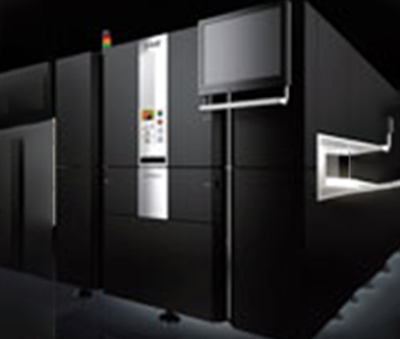
Product brand: OMRON Omron
Product model: OMRON VT-X700/X-RAY
Origin: Japan
OMRON VT-X700/X-RAY : In recent years, in the automotive electronics industry, consumer electronics industry, and digital home appliance industry, in addition to the requirements for size, multi-function, high performance, etc., more and more manufacturers have Increased high-density component placement.
The mounting substrates assembled into finished products also use a large number of components such as BGA/CSP whose solder joint surfaces cannot be seen on the surface. In the past, X-ray fluoroscopy inspection methods caused many misjudgments and missed diagnoses, making the inspection results extremely unstable.
Omron VT-X700/X-RAY solves the practical problems of your SMT production line:
1: High reliability
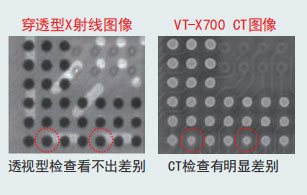
Omron VT-X700/X-RAY uses CT tomography to detect shapes that cannot be detected by penetrating X-ray devices or visual inspection, such as the solder joint surface of BGA components. Quality judgment can be achieved.
2: high speed
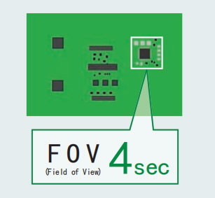
The inspection time of one FOV only takes 4 seconds, achieving high-speed inspection.
3: Omron VT-X700/X-RAY is safe and secure
Safe, the leakage of X-rays is less than 0.5μSv/h. X-rays are emitted in pulse mode only when needed, which not only reduces the amount of radiation emitted, but also extends the service life of internal components.
Omron VT-X700/X-RAY performance features:
High-speed X-ray CT tomography automatic inspection device
model: VT-X700-E, VT-X700-L
Omron VT-X700/X-RAY, a high-speed CT tomography X-ray inspection device that supports mass production online full inspection
Omron VT-X700/X-RAY working mode:
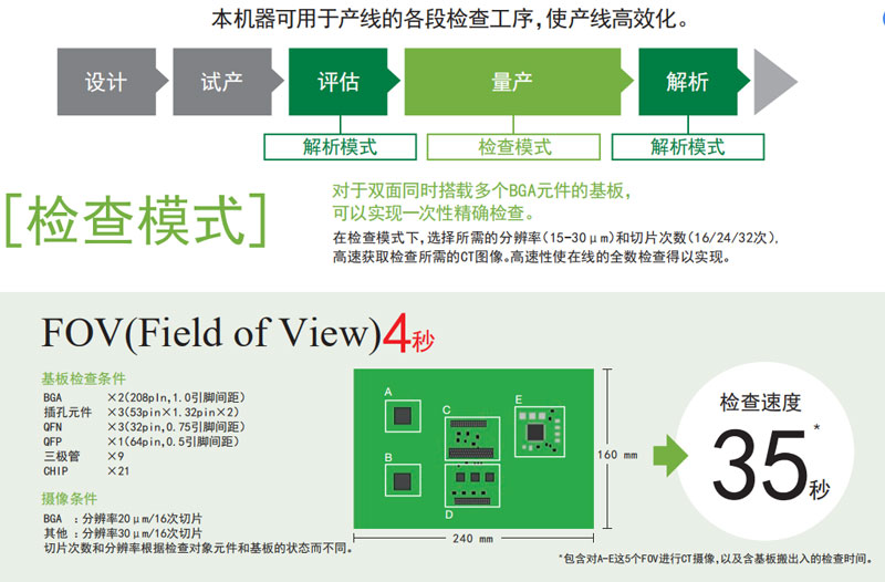
Omron VT-X700/X-RAY analysis mode:
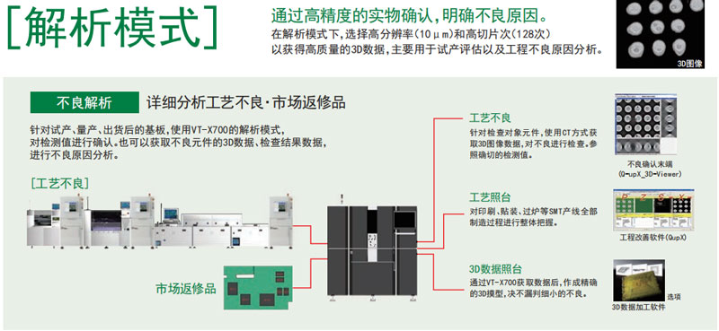
Omron VT-X700/X-RAY technical parameters:
project | content | ||
Model | VT-X700-E VT-X700-L | ||
Check object component | BGA/CSP, plug-in components, SOP/QFP, transistors, CHIP components, bottom electrode components, QFN, power modules | ||
Check item | Missing solder, non-wetting, amount of solder, offset, foreign matter, bridge, presence of pins, etc. (different selections are made according to the inspection objects) | ||
Camera specifications | Camera method | 3D slice imaging with parallel CT | |
Camera resolution | 10.15, 20, 25, 30 m (can be selected according to different inspection objects) | ||
X-ray source | Sealed micro focusing X-ray tube (130KV) | ||
X-ray sensor | FPD | ||
Target substrate | Substrate size | Corresponding substrate (50×50-330×305mm) thickness: 0.4-3.0mm | Corresponding substrate (50×50-610×610mm) thickness: 0.6-7.0mm |
Board weight | 2.0kg or less (components mounted) | 12.0kg or less (components mounted) | |
Mounted component height | Surface: below 50mm | Reverse: 20mm or less | |
Plate bending | 2.0mm or less | Below 3.0mm | |
Machine specifications | Dimensions | 1.550 (W) X1.650 (D) X1.620 (H) mm | 2.180(W) X2.500(D)×1.720(H)mm |
Device weight | About 2.920kg | About 5,250kg | |
Substrate transfer height | 900±15mm | ||
voltage | Single phase 200/210/220/230/240VAC(±10%),50/60Hz | 3 | |
power | 3.1kVA | 4.7kVA | |
x-ray leakage | Less than 0.5 uSv/h | ||
135 1032 1270
Contact: Miss Jiang
Mail box: market@topsmt.com
Address: 201, Building 4, Innovation Port, Hanyu Bay, Fuhai Street, Baoan District, Shenzhen
Please submit your request and we will call you right back

